(China (Mainland))


Product Summary
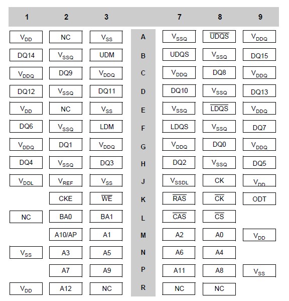
The K4N51163QZ-HC25 is a 512Mb gDDR2 SDRAM chip. It is organized as 8Mbit x 16 I/O x 4banks banks device. The K4N51163QZ-HC25 achieves high speed graphic double-data-rate transfer rates of up to 500MHz for general applications. The chip is designed to comply with the following key gDDR2 SDRAM features such as posted CAS with additive latency, write latency = read latency - 1, Off-Chip Driver(OCD) impedance adjustment and On Die Termination. The K4N51163QZ-HC25 is available in 84ball FBGAs.
Parametrics
K4N51163QZ-HC25 absolute maximum ratings: (1)VDD Voltage on VDD pin relative to VSS: - 1.0 V to 2.3 V; (2)VDDQ Voltage on VDDQ pin relative to VSS: - 0.5 V to 2.3 V; (3)VDDL Voltage on VDDL pin relative to VSS: - 0.5 V to 2.3 V; (4)VIN, VOUT Voltage on any pin relative to VSS: - 0.5 V to 2.3 V; (5)TSTG Storage Temperature: -55 to +100 ℃.
Features
K4N51163QZ-HC25 features: (1)1.8V ±0.1V power supply for device operation; (2)1.8V ±0.1V power supply for I/O interface; (3)Write Latency (WL) = Read Latency (RL) -1; (4)Burst Legth: 4 and 8 (Interleave/nibble sequential); (5)Programmable Sequential/ Interleave Burst Mode; (6)Bi-directional Differential Data-Strobe(Single-ended data-strobe is an optional feature); (7)Off-chip Driver (OCD) Impedance Adjustment; (8)On Die Termination; (9)Refresh and Self Refresh; (10)Lead - Free and Halogen - Free 84 ball FBGA (RoHS compliant).
Diagrams
 |
 K4N56163QF-GC |
Other |
|
Data Sheet |
Negotiable |
|
||||
|
K4N51163QC-ZC |
Other |
|
Data Sheet |
Negotiable |
|
||||