(China (Mainland))

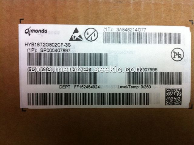
Product Summary
The HYB18T2G802CF-3S is a 2-Gbit Dual Die Double-Data-Rate-Two SDRAM. Each 1-Gbit device is organized as 32 Mbit × 4 I/O × 8 banks or 16 Mbit × 8 I/O × 8 banks chip. The HYB18T2G802CF-3S achieves high speed transfer rates starting at 400 Mb/sec/pin for general applications. It is available in TFBGA package.
Parametrics
HYB18T2G802CF-3S absolute maximum ratings: (1)VDD voltage on VDD pin relative to VSS: -1.0 to 2.3 V; (2)VDDQ voltage on VDDQ pin relative to VSS: -0.5 to 2.3 V; (3)VDDL voltage on VDDL pin relative to VSS: -0.5 to 2.3 V; (4)VIN, VOUT voltage on any pin relative to VSS: -0.5 to 2.3 V; (5)TSTG storage temperature: -55 to 100 ℃.
Features
HYB18T2G802CF-3S features: (1)DRAM organizations with 4.8 data in/outputs; (2)Double data rate architecture; (3)Programmable CAS latency: 3, 4, 5 and 6; (4)Programmable burst length: 4 and 8; (5)Differential clock inputs(CK and CK); (6)Bi-directional differential data stobes are transmitted/received with data. Edge aligned wit read data and center-aligned with write data; (7)DLL aligns DQ and DQS transitions with clock; (8)DQS can be disabled for single-ended data strobe operation; (9)Data mask for write data.
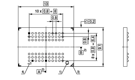
Diagrams
 |
 HYB15T1G160C2F-2.5 |
Other |
|
Data Sheet |
Negotiable |
|
||||
|
HYB15T1G160C2F-25F |
Other |
|
Data Sheet |
Negotiable |
|
||||
|
HYB15T1G160C2F-3S |
Other |
|
Data Sheet |
Negotiable |
|
||||
|
HYB15T1G400C2F-2.5 |
Other |
|
Data Sheet |
Negotiable |
|
||||
|
HYB15T1G400C2F-25F |
Other |
|
Data Sheet |
Negotiable |
|
||||
|
HYB15T1G400C2F-3.7 |
Other |
|
Data Sheet |
Negotiable |
|
||||