(China (Mainland))

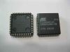
Product Summary
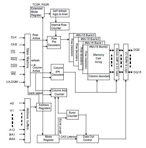
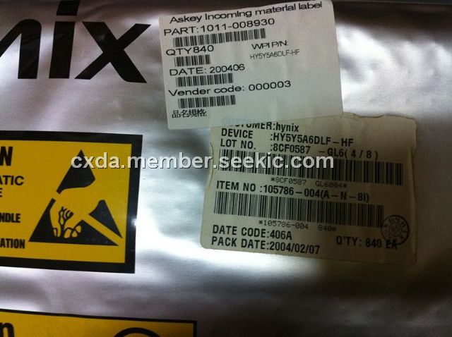
The HY5Y5A6DLF-HF is a Low Power SDRAM is suited for non-PC application which uses the batteries such as PDAs, 2.5G and 3G cellular phones with internet access and multimedia capabilities, mini-notebook, handheld PCs. The HY5Y5A6DLF-HF is a 268,435,456bit CMOS Synchronous Dynamic Random Access Memory. It is organized as 4banks of 4,194,304x16. The HY5Y5A6DLF-HF provides for programmable options including CAS latency of 1, 2, or 3, READ or WRITE burst length of 1, 2, 4, 8, or full page, and the burst count sequence(sequential or interleave).
Parametrics
HY5Y5A6DLF-HF absolute maximum ratings: (1)Ambient Temperature TA: -25 ~ 70 ℃; (2)Storage Temperature TSTG: -55 ~ 125 ℃; (3)Voltage on Any Pin relative to VSS VIN, VOUT: -1.0 ~ 4.6 V; (4)Voltage on VDD relative to VSS VDD: -1.0 ~ 4.6 V; (5)Voltage on VDDQ relative to VSS VDDQ: -1.0 ~ 4.6 V; (6)Short Circuit Output Current IOS: 50 mA; (7)Power Dissipation PD: 1 W; (8)Soldering Temperature . Time TSOLDER: 260 · 10 ℃ · Sec.
Features
HY5Y5A6DLF-HF features: (1)Standard SDRAM Protocol; (2)Internal 4bank operation; (3)Voltage: VDD = 3.0V & 3.3V, VDDQ = 3.0V & 3.3V; (4)LVCMOS compatible I/O Interface; (5)Low Voltage interface to reduce I/O power; (6)Low Power Features; (7)CAS latency of 1, 2, or 3; (8)Packages : 54ball, 0.8mm pitch FBGA; (9)-25 ~ 70℃ Operation.
Diagrams